


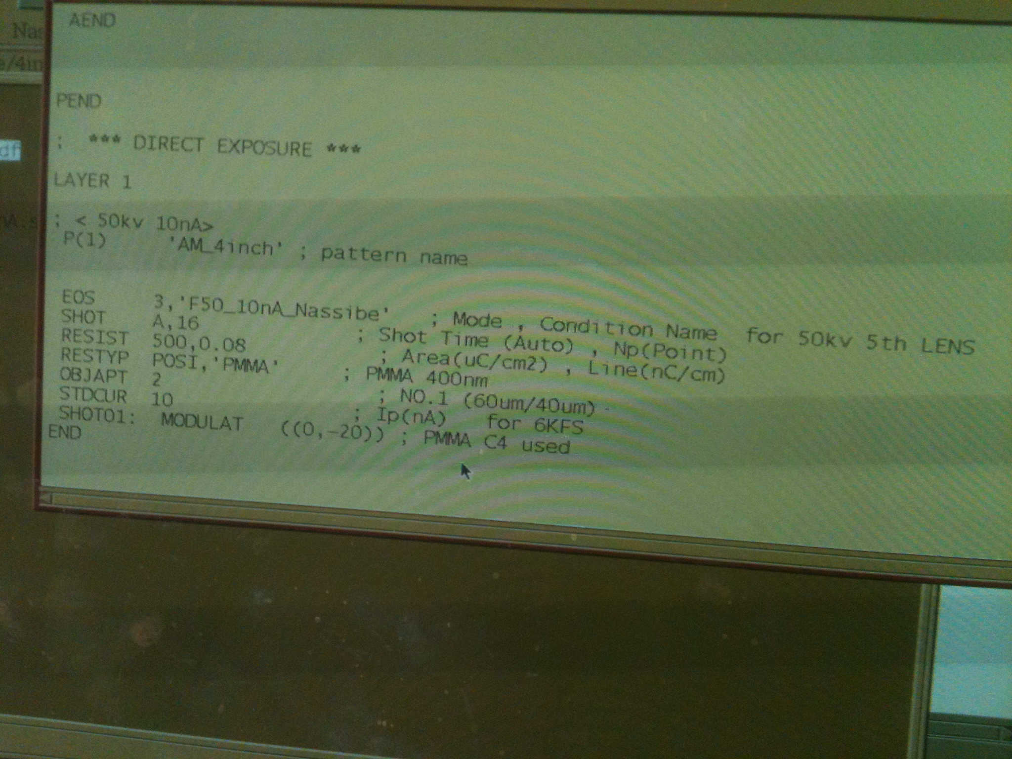
Direct writing of complex patterns down to 20nm scale,
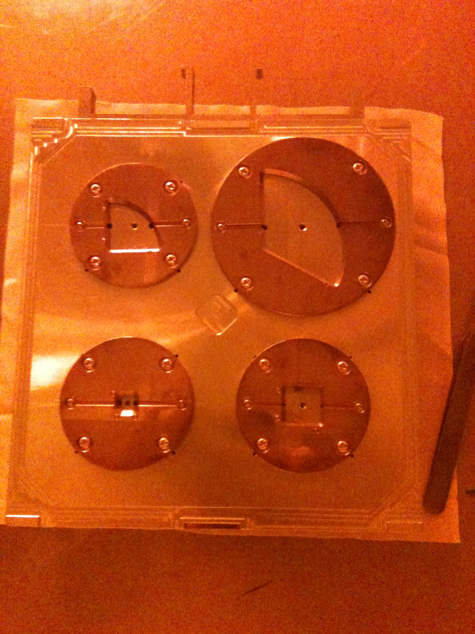
Mask making on quartz substrate coated with Chromium.
on 4”-8” wafers and pieces coated with sensitive polymer
Features: Finely focused beam of electrons - Electrons accelerated at 50keV
Point beam, Gaussian in distribution, vector scanned over the desired area, stage stationary during the writing operation
Exposure conditions:
EOS 7,'U50_100pA_User6_07082009' ; Mode, Condition Name for 50kv 5th LENS;
SHOT A,4 ; Shot Time (Auto) , Np (Point);
RESIST 180,0.12 ; ZEP 520 Area (uC/cm2) , Line (nC/cm);
RESTYP POSI,'ZEP-520' ;ZEP 520;
OBJAPT 1 ; NO.1 (60um/40um);
STDCUR 0.1 ; Ip(nA) for 6000FS;
SHOT01: MODULAT((0,-41))
EOS 3,'F50_1nA_Ap2_User9_10302008' ; Mode, Condition Name for 50kv 4th LENS;
SHOT A,2 ; Shot Time (Auto) , Np (Point);
RESIST 180,0.12 ; ZEP 520 Area (uC/cm2) , Line (nC/cm);
RESTYP POSI,'ZEP-520' ;ZEP 520;
OBJAPT 2 ;
STDCUR 1.0 ; Ip(nA) for 6000FS;
SHOT01: MODULAT((0,-40)) ; (0,-20) was also used
EOS 3,'F50_15nA_Ap2_User9_10302008' ; Mode, Condition Name for 50kv 4th LENS;
SHOT A,12 ; Shot Time (Auto) , Np (Point);
RESIST 180,0.12 ; ZEP 520 Area (uC/cm2) , Line (nC/cm);
RESTYP POSI,'ZEP-520' ;ZEP 520;
OBJAPT 2 ;
STDCUR 15.0 ; Ip(nA) for 6000FS;
SHOT01: MODULAT((0,-28))
EOS 3,'F50_3nA_Ap2_User9_10302008' ; Mode, Condition Name for 50kv 4th LENS;
SHOT A,8 ; Shot Time (Auto) , Np (Point);
RESIST 20,0.1 ;
RESTYP NEG,'NEB31A3' ;
OBJAPT 2 ;
STDCUR 3 ; Ip(nA) for 6000FS;
SHOT01: MODULAT((0,-68))
EOS 7,'U50_100pA_User9_05142009' ; Mode, Condition Name for 50kv 5th LENS;
SHOT A,2 ; Shot Time (Auto) , Np (Point);
RESIST 500, 0.8 ;
RESTYP POSI,'PMMA' ;
OBJAPT 1 ; NO.1 (60um/40um);
STDCUR 0.1 ; Ip(nA) for 6000FS;
SHOT01: MODULAT((0,-20))
EOS 3,'F50_1nA_Ap2_User9_10302008' ; Mode, Condition Name for 50kv 4th LENS;
SHOT A,4 ; Shot Time (Auto) , Np (Point);
RESIST 500, 0.8 ;
RESTYP POSI,'PMMA' ;
OBJAPT 2 ;
STDCUR 1.0 ; Ip(nA) for 6000FS;
SHOT01: MODULAT((0,-28)
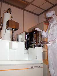
1. Loading wafers. Check the status of the Autoloader load lock to make sure that the system is under proper vacuum and the Valve is closed. Move loader to initial position. Push the red vent button next to the load lock. When vented open the door to the proper position and move lever located to the left on the lower base to the up position. This will lock the door in place. Lower lever in front then rotate the wafer holder Lock to the closed position. Slowly pull out the assembly until it latches in place. Move the wafer holder lock to the open position and remove the wafer chuck that you plan to use. After wafer has been properly placed in wafer holder slide back in carriage and lock in place. Unlatch Carriage and slide into load lock. Latch lever in front of carriage then rotate the wafer holder lock to the open position. Move the lever located on the lower base to the down position close door and latch lever. Release red vent button, the light should blink. Watch the right penning gauge to verify the pressure it should be in the lower range and well below the white arrow.
2 Transfer of wafers. When you have sufficient vacuum in the load lock chamber. Move elevator to the position of the wafer. Check to see that the status light is extinguished before going further. Open slot valve (VI) check status then hit transfer button Check status then close valve. You are ready for to move on to the calibration step.
3 Calibration and exposure. Open the Calibration menu. First you need to run Eosset to set the initial exposure settings. This will load the previous settings from a prior run. Be sure to check Demag and Restor then Run Cancel. Stgcom is used to move the stage to the correct position for calibration and orientation. First step is to move stage so the beam is centered in the faraday cup. Hit select then select faraday cup then click move.
When the beam is centered in the Faraday cup hit blanking off and check the current reading on screen. Hit button G-AL and use the left 2 knobs to peak the reading in the cup then 2/3 lens 3 demag 2/3 lens 2 demag. Then set the current value to specifications.
Focus on a spot ( BEI is fine for higher resolutions ) and deselect lens mode set to wobble and select 5th lens mode. Adjust Aperture to obtain as little shifting of image as possible. Try a mag setting of 4x10 -4 to 1x10 -5 and the scan speed set to 0.0 . Deselect 5th lens mode and press Clr.
Recheck gun alignment after wobbler to make sure nothing has changed.
Move to SEM sample position and focus on sample SEI mode 1st . This will get you in the ballpark when you start your focusing on the wafer at a later step. Set to BEI mode and adjust focus to minimize pulling. Adjust astigmatism to resolve lines between gold and recheck focus.
For 5th lens 100 pa the focus settings are initially around 30500." Move to center position of wafer and hit COL1 then turn off blanking for approx 10 seconds. Turn blanking back on. Focus on sample until you see a sharp dot. On the 8” wafer the focus is slightly different. Set focus to around 30900. Create a beam spot on the wafer using Col 1 and Blanking. The final results should be at 1 x 10 5, you should be sharply focused with the dot size no bigger than 1 square.
Run INIMSH this is your initial alignment for your stage coordinates. Run until you get lowest numbers.
If signal takes up more than 1 to 1 _ boxes run MDAGC. Run INIMSH again. Run PDEF. Run DISTOR. Execute it will prompt write to menu hit ok. Now you need to save all your calibrations. Hit save Then Edit parameters Acquisition of latest status. It will prompt you to save. Hit save then cancel. Go to expose pick out your mag file that you previously compiled from your JDF and SDF files and pattern data. Highlight then hit expose.